Pinout
The ATmega32u4 microcontroller has all the serial peripherals you would expect from a modern MCU, a full-speed USB connection and a generous number of ADC inputs. The image below shows all of the GPIO port and pin numbers of the MCU and the commonly used "Alternate functions" of each pin. The following sections below will describe in detail each category of pin funtions.
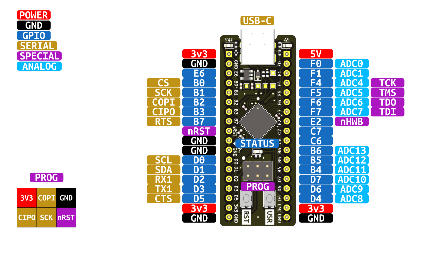
All GPIO and serial peripherals (except USB) operate at 3.3V. Level translators should be used when interfacing with other systems that may run at 1.8V or 5V
Power & GND
The ATmega32u4 breakout board is capable of being powered in two ways:
- The first being to connect a USB type C cable to the USB connector. This supplies 5V to the on board linear voltage regulator which
then provides a 3.3V rail to the microcontroller. When connecting a USB cable 5V is also made availabe on the
5Vpin header pin. - The second method is to provide 5V to the
5Vpin. This will then supply the on board regulator which powers the 3v3 power rail. It is OK to use this method at the same time as plugging in a USB cable. A diode is in place to prevent back-feeding the 5V power rail into the USB connector.
Regardless of which method you choose to power the board, the 3.3V rail will be made available on the 3v3 pins.
It is not recommended to supply 3.3V to the 3v3 pins as it could damage the on board linear voltage regulator.
GPIO
Every GPIO can be used for reading in or writing out a signal and some also have the ability to trigger interrupts on Rising or Falling edges when configured as an input.
The naming convention is [PORT_LETTER][PIN_NUMBER] - for example D5 is port D, pin 5.
Status LEDs
The breakout board has three on board status LEDs.
- 5V LED: Indiciates the status of the 5V rail
- 3.3V LED: Indicates the status of the 3.3V rail
- Status LED: General purpose LED that can be used in the user application. This LED is driven via the
D4GPIO.
Clock
The breakout board has an on-board 16MHz crystal giving a final CORE_FREQ of 16MHz
USB
USB Full-Speed capable of synchrounous serial communication at a frequency of 12MHz
TWI
Two Wire Interface or I2c supports half-duplex serial communication to a max of 128 peripherals on a reduced two wire interface at a max frequency of 400kHz
SCL / D0: Serial Clock or GPIOD0SDA / D1: Serial Data or GPIOD1
USART
Universal Synchronous and Asynchronous Receiver and Transmitter supports full-duplex serial communication with hardware flow-control support
TX1 / D3: Transmit line or GPIOD3RX1 / D2: Receive line or GPIOD2CTS / D5: Flow Control - Clear to Send or GPIOD5RTS / B7: Flow Control - Request to Send or GPIOB7
SPI
Serial Peripheral Interface supports full-duplex serial communication to one or more peripherals at a max frequnecy of CORE_CLOCK_FREQ / 2 MHz
COPI / B2: Controller Out - Peripheral In or GPIOB2CIPO / B3: Controler In - Peripheral Out or GPIOB3SCK / B1: Serial Clock or GPIOB1CS / B0: Chip Select or GPIOB0
The CS pin does not have to be used when utilizing the SPI peripheral. The user can instead manually actuate a GPIO pin connected to a peripherals CS line.
This allows for a larger bus and more peripherals to be connected at once.
Analog
The breakout board has twelve 10-bit ADC, or Analog to Digital Converter, pins. Each capable of reading in voltage ranges from 0 to 3.3V giving a reading accuracy down to ~3mV.
ADC0 / F0: Analog input 0 or GPIOF0ADC1 / F1: Analog input 1 or GPIOF1ADC4 / F4: Analog input 4 or GPIOF4ADC5 / F5: Analog input 5 or GPIOF5ADC6 / F6: Analog input 6 or GPIOF6ADC7 / F7: Analog input 7 or GPIOF7ADC8 / D4: Analog input 8 or GPIOD4ADC9 / D6: Analog input 9 or GPIOD6ADC10 / D7: Analog input 10 or GPIOD7ADC11 / B4: Analog input 11 or GPIOB4ADC12 / B5: Analog input 12 or GPIOB5ADC13 / B6: Analog input 13 or GPIOB6
Special and Programming
The special pins are generally used for programming the device via JTAG or USB DFU and are as follows
nRST: Active Low chip resetnHWB: Active Low hardware boot. Used in conjuction withnRSTto jump to the built-in bootloaderTCK: JTAG ClockTMS: JTAG Test Mode SelectTDO: JTAG Test Data OutTDI: JTAG Test Data In
AVR-SPI PROG header
A dedicated programming header is available on the breakout board which matches the AVR-SPI standard programming pinout. These SPI pins are the same signals
found down the left side of the board on GPIOs B1 - B3